|
ESD China |
English 繁体 | 最近信息 | 静电产品 | 静电标准 | 培训服务 | ESD专家 | 静电应用 | 静电测量 | ESD防护 |
业务: |
|
业务: |
|
|
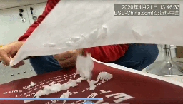
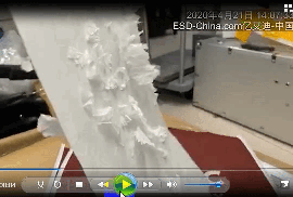
EST712C静电驻极N95口罩布熔喷布无纺布静电驻极机静电驻极棒 (高效、易安装)
|
2001 EOS/ESD Symposium, Portland, OR Table of Contents Session 1A: Novel CMOS Devices Moderator: Tim Maloney, Intel Corporation 1A.1 Multi-Finger Turn-on Circuits and Design Techniques for Enhanced ESD Performance and Width-Scaling, M.P.J. Mergens, C.C. Russ, J. Armer, P.C. Jozwiak, G. Kolluri, L.R. Avery, Sarnoff Corporation; K.G. Verhaege, Sarnoff Europe, p1. 1A.2 5-V Tolerant Fail-Safe ESD Solutions for a 0.18um Logic CMOS Process, K. Kunz, C. Duvvury, H. Shichijo, Texas Instruments, Inc., p12. 1A.3 GGSCRS: GGNMOS Triggered Silicon Controlled Rectifiers for ESD Protection in Deep Sub-Micron CMOS Processes, C. Russ, M.P.J. Mergens, J. Armer, P.C. Jozwiak, G. Kolluri, L.R. Avery, Sarnoff Corporation; K.G. Verhaege, Sarnoff Europe, p22. 1A.4 ESD Protection Design for Mixed-Voltage 1/0 Buffer by Using Stacked-NMOS Triggered SCR Device, M.D. Ker, C-H Chuang, National Chiao-Tung University, H-C Jiang, Industrial Technology Research Institute, p32. Moderator: Donn Bellmore, Universal Instruments Corporation IB.1 An Analysis of ESD Packaging Systems Through Thermoforming, J. Allen, VPI Mirrex Corporation, p44.1B.2 Performance of Fiber Based ESD Protective Packaging, J. Paasi, R. Vuorinen, P. Maijala, H. Paimen, VTT Automation; V. Salminen, Nokia Networks,p50. 1B.3 PAPERWITHDRAWN, p55. 1B.4 New ESD Control Material Based on Special Carbon, N. Nishihata, Kureha Chemical Industry Co., Ltd., p56. Session 2A: Simulation and Modeling Moderator: Markus Mergens, Sarnoff Corporation 2A.1 Analysis and Improved Compact Modeling of the Breakdown Behavior of Sub-0.25 Micron ESD Protection ggNMOS Devices, V. Vassilev, H. Maes, IMEC, KUL, ESAT; M. Lorenzini, G. Groeseneken, IMEC; M. Steyaert, KUL, ESAT, p62.2A.2 Modeling Substrate Diodes under Ultra High ESD Injection Conditions, G. Boselli, University of Twente, Texas Instruments, Inc., S. Ramaswamy, A. Amerasekera, Texas Instruments, Inc.; T. Mouthaan, University of Twente; F. Kuper, University of Twente, Philips Semiconductors Nijmegen, p71. 2A.3 Modular, Portable, and Easily Simulated ESD Protection Networks for Advanced CMOS Technologies, C.A. Torres, J.W. Miller, M. Stockinger, M.D. Akers, M.G. Khazhinsky, J.C. Weldon, Motorola, Inc., p82. 2A.4 Automatic Layout Based Verification of Electrostatic Discharge Paths, P. Nagan, D. Oliver, T. Smedes, Philips Semiconductors; R. Gramacy, University of California; C-K Wong, Kestrel Solutions, p96. 2A.5 Experimental Analysis and Electro-Thermal Simulation of Low-and High-Voltage ESD Protection Bipolar Devices in a Silicon-on-Insulator Bipolar-CMOS-DMOS Technology, R. Depetro, A. Andreini, C. Contiero, ST-Microelectronics; F. Mignoli, G. Meneghesso, E. Zanoni, University of Padova, p102. 2A.6 Human Body Model Test of a Low Voltage Threshold SCR Device: Simulation and Comparison with the Transmission Line Pulse Test, A. Guilhaume, EADS CCR, CEGELY; B. Foucher, EADS CCR, J.P. Chante, CEGELY; P. Galy, Pote Universitaire Leonard De Vinci; S. Bardy, F. Blanc, Philips Semiconducteurs, p110. Moderator: Rick Rodrigo. SIMCO 2B.1 Controlling ESD Damage of lCs at Various Steps of Back-End Process, J. Marley, D. Tan, Xilinx, Inc.; V. Kraz, Credence Technologies, Inc., p1202B.2 An Effective ESD Protection System in the Back End (BE) Semiconductor Manufacturing Facility, K-P Yan, R. Gaertner, S. Lim, lnfineon Technologies (Malaysia) Sdn. Bhd., p125. 2B.3 Preparing a Microelectronics Assembly and Test Area for More Sensitive Product, T. Lesniewski, S. Hartooni, TRW Space & Electronics Group-, E. Kaully, Kulicke & Soffa Industries, Inc. p133. 2B.4 Anodized Aluminum Alloys, Insulator or Not?, D.G. Bellmore, Universal Instruments Corporation, p141. 2B.5 DC Transient Monitoring and Analysis to Prevent EOS in Burn-in Systems, Y. Jaimsomporn, S. Phunyapinuant, W. Tan, Advanced Micro Devices, p149. 2B.6 Measurement of Electrostatic Generation in Semiconductor Processing Fluids as a Result of Pumping Through lnsulative Pumps and Tubing, C. Newberg, River's Edge Technical Service, p153. Session 2C: Magnetic Recording Heads I Moderator: Eric Granstrom, Seagate Technology 2C.1 Field-induced Charging and FIM ESD Tests on GMR Heads in Hard Disk Assembly, B-C Yap, Western Digital (Malaysia) Sdn. Bhd.; J. Turangan, Western Digital, p160.2C.2 A Study of Shunt ESD Protection for GMR Recording Heads, A. Wallash, Maxtor Corporation, p167. 2C.3 Field Emission Noise Caused by Capacitance Coupling ESD in AMR/GMR Heads, T. Ohtsu, H. Yoshida, N. Hatanaka, Hitachi, Ltd,. p172. 2C.4 A Study of GMR Read Sensor Induced by Soft ESD Using Magnetoresistive Sensitivity Mapping (MSM), S.T. Hung, C.Y. Wong, The Hong Kong University of Science & Technology; M. Osborn, Digital Instruments, J. Kagaoan, L.Z. Zhang, R. Bordeos, Shenzhen Kaifa Technology Co. Ltd., p175. 2C.5 Using PSPICE to Study Transient Propagation in GMR Circuits, J. Himle, Maxtor Corporation, p182. 2C.6 Effect of Low-Level ESD on the Lifetime of GMR Heads, I-F Tsu, M. Davis, C. Chang, Seagate Technology, p187. Moderator: Robert Ashton, Agere Systems 3A.1 Invited Paper: Interconnect Reliability Under ESD Conditions: Physics, Models and Design Guidelines, K. Banerjee, Stanford University, p191. (Paper Not Available at Press Time)3A.2 Development of Substrate-Pumped NMOS Protection for a 0.13um Technology, C. Salling, J. Hu, J. Wu, C. Duvvury, R. Cline, R. Pok, Texas Instruments, Inc., p192. 3A.3 Evaluation of Diode-Based and NMOS/Lnpn-Based ESD Protection Strategies in a Triple Gate Oxide Thickness 0.13um CMOS Logic Technology, R. Gauthier, M. Muhammad, C. Putnam, IBM Microelectronics Semiconductor Research and Development Center; W. Stadler, K. Esmark, P. Riess, Infineon Technologies AG-, A. Salman, George Mason University, p205. 3A.4 Study of Trigger Instabilities in Smart Power Technology ESD Protection Devices Using a Laser lnterferometric Thermal Mapping Technique, D. Pogany, M. Litzenberger, P. Kamvar, E. Gornik, Vienna University of Technology; C. Furbok, Vienna University of Technology (now with Austria Microsystems) G. Groos, K. Esmark, H. Gossner, M. Stecher, Infineon Technologies, p216. 3A.5 Using Thin Emitters to Control BVceo Effects in Punch-Through Diodes for ESD Protection, R. van Dalen, G.A.M. Hurkx, M.A.A. in't Zandt, E.A. Hijzen, Philips Research Leuven; P.J.W. Weijs, A. den Dekker, Philips Semiconductors, p228. 3A.6 Human Body Model, Machine Model, and Charged Device Model ESD Testing of Surface Micromachined Microelectromechanical Systems (MEMS), J.A. Wairaven, J.M. Soden, E.I. Cole, Jr., D.M. Tanner, R.E. Anderson, Sandia National Laboratories, p238. 3A.7 Electrostatic Discharge and Electrical Overstress on GaN/InGaN Light Emitting Diodes, G. Meneghesso, A. Chini, A. Maschietto, E. Zanoni, University of Padova; P. Malberti, M. Ciappa, Swiss Federal Institute of Technology (ETH), p249. Moderator: Steve Koehn, 3M Company 3B.1 Recent Innovations of Inherently Conducting Polymers for Optimal (106 - 109 OHM/SQ) ESD Protection Materials, S.J. Dahman, RTP Company, p255.3B.2 The Purity, Wetting, and Electrical Properties of Static-Dissipative Surfactant Coatings Versus Inherently-Dissipative Polymer Alloys, R.M. Bucha, Entegris, Inc.-, M. Acevedo, SurfStat, Inc., p262. 3B.3 A Study of the Variables of Electrodes Used in the Measurement of Table and Floor Materials and How They Affect the Test Results, H. Berndt, B.E.STAT, p267. 3B.4 Electronic Part Damage by Antistat Vapor, J.M. Kolyer, A.A. Passchier, W.G. Peterson, The Boeing Company, p272. 3B.5 A Study of the Electrical Properties of Polymeric Materials Used for Gloves and Finger Cots, C. Newberg, River's Edge Technical Service, Inc.; B. Baumgartner, ESD West; G. Chase, S. Weitz, ETS, Inc.; W. Casselman, QRP Incorporated; A. Hartkopf, Ansell Healthcare; T. Jarrett, Guidant, Corp.; W.J. Metz, Hewlett Packard; R.D. Rodrigo, SIMCO; J. Turangan, Western Digital, J. Vaughn, BF Goodrich, p281. 3B.6 Contact Transfer of Anions from Hands as a Function of the Use of Hand Lotions, R.W. Welker, M. Schulman, Jet Propulsion Laboratory, p288. Session 3C: Magnetic Recording Heads II Moderator: Jenny Himle, Maxtor Corporation 3C.1 Transmission Line Pulse (TLP) Testing of GMR Recording Heads, A. Wallash, Maxtor Corporation, p291.3C.2 A Study of GMR Breakdown Damage in Cleaning, F. Deng, Z.Y. Teng, W. Li, R. Tao, SAE Magnetics (HK), Ltd., p295. 3C.3 Voltage Raised in AL2O3 Gap of GMR Head in the Deshunting Process, A. Siritaratiwat, N. Suwannata, Khon Kaen University; J. Pinnoi, C. Pupaichitkul, Seagate Technology (Thailand) Ltd., p299 3C.4 PAPER WITHDRAWN, p305 3C.5 Wafer Charging Evaluation Method of Ion Milling in GMR Head Manufacturing Using Antenna Test Element Group, S. Kakuta, H. Taniguchi, A. Kondo, H. Ikeda, K. Furusawa, S. Todoroki, Hitachi, Ltd., p306. 3C.6 ESD Audit Limits and Actual Damage Thresholds: A Theoretical Analysis, B. Perry, Maxtor Corporation, p311. 3C.7 GMR Heads as ESD Detectors-A Direct Assessment of Subtle ESD, J.S. Luo, C-Y Yeh, A. Sanayei, IBM, p318. Session 4A: RF ESD Design and Technology Moderators: Richard Ida, Motorola, and Eugene Worley, Conexant Systems 4A.1 Invited Paper: The Future of RF Technology for Established Wireless Markets and Emerging Wireless Applications, D.R. Pehlke, Ericsson, Inc.,p322.4A.2 Silicon Germanium Heterojunction Bipolar Transistor ESD Power Clamps and the Johnson Limit, S. H. Voldman, A. Botula, IBM Communications Research and Development Center; D. T. Hui, IBM Corporation; P. A. Juliano, University of Illinois at Urbana-Champaign, p326. 4A.3 Diode Network Used as ESD Protection in RF Applications, R.M.D.A. Veighe, Philips Semiconductors Nijmegen (now with Philips Research Leuven); P.W.H. de Vreede, P.H. Woerlee, Philips Research Laboratories Eindhoven, p337. 4A.4 ESD Protection Design for CMOS RF Integrated Circuits, M-D Ker, T-Y Chen, National-Chiao-Tung University; C-Y Chang, Industrial Technology Research Institute, p346. 4A.5 Analysis and Optimization of Distributed ESD Protection Circuits for High-Speed Mixed-Signal and RF Applications, C. Ito, K. Banerjee, R.W. Dutton, Stanford University, p355. 4A.6 Influence of Process and Device Design on ESD Sensitivity of a Silicon Germanium Heterojunction Bipolar Transistor, S.H. Voldman, L.D. Lanzerotti, R.A. Johnson, IBM Communications Research and Development Center, p364. Moderator: Douglas Smith, D. C. Smith Consultants4B.1 Broadband Measurement of ESD Risetimes to Distinguish between Different Discharge Mechanisms, S. Bonisch, W. Kalkner, Technical University Berlin; D. Pommerenke, Hewlett Packard, p373. 4B.2 The EMI/ESD Environment of Large Server Installations, D.C. Smith, D.C. Smith Consultants; M. Hogsett, Ion Systems, p385. 4B.3 Comparison of Solutions to Minimize Voltages Induced by ESD Events on Adjacent Microstrips, J. Harris, Littelfuse, Inc., p390. 4B.4 Improving the Balanced Coaxial Differential Probe for High-Voltage Pulse Measurements, T.J. Maloney, D-H Cho, S.S. Poon, B. Lisenker, Intel Corporation, p398. 4B.5 Development of an Experimental Platform to Study the Effect of Speed of Approach on the Electrostatic Discharge (ESD) Event, W.D. Greason, Z. Kucerovsky, C. Zaharia, University of Western Ontario, p408. 4B.6 Electromagnetic Field Generated by Transient Electrostatic Discharges (ESD) from Person Charged with Low Electrostatic Voltage, J. Huang, Q. Deng, F. Liu, Z. Chen, P. Liu, Beijing Research Institute of Special Electromechanical Techniques, p415. Session 4C: Transmission Line Pulsing and Standardization Moderator: Mike Chaine, Micron Technology, Inc. 4C.1 Invited Paper: ESD Evaluation by TLP Method on Advanced Semiconductor Devices, K. Kato, Y. Fukuda, OKI Electric Industry Co., Ltd., (Best Paper RCJ 2000 EOS/ESD Symposium, Japan), p419.4C.2 The Application of Transmission Line Pulse Testing for the ESD Analysis of Integrated Circuits, T. Smede-s, R.S. Ruth, A.J. Huitsing, Philips Semiconductors; R.M.D.A Velghe, Philips, Semiconductors, Philips Research Leuven, p426. 4C.3 Characterization of a 0.16um CMOS Technology using SEMATECH ESD Benchmarking Structures, R.A. Ashton, Y. Smooha, Agere Systems, p435. 4C.4 Integration of TLP Analysis for ESD Troubleshooting, L-M Ting, C. Duvvury, 0. Trevino, J. Schichl, T. Diep, Texas Instruments, p445. 4C.5 Correlation Considerations: Real HBM to TLP and HBM Testers, J.Barth, J. Richner, Barth Electronics, Inc., p453. 4C.6 Contributions to Standardization of Transmission Line Pulse Testing Methodology, B. Keppens, V. De Heyn, M. Natarajan lyer, G. Groeseneken, Imec vzw, p461. Workshop Chair: Dale Parkin, IBM A.1 ESD in Magnetic Recording, Moderator: Eric Granstrom, Seagate Technology, p469 A.2 ESD Control Program - Audit Problems, Moderator: Bill Metz, Hewlett Packard, p470. A.3 On-Chip Protection, Moderator: Eugene Worley, Conexant Systems, p471. A.4 How and Why TLP is Used, ModeratoC Jon Barth, Barth Electronics, Inc., p472. Workshop Chair: Dale Parkin, IBM B.1 System Level ESD Considerations, Moderator: Douglas Smith, D.C. Smith Consultants, p473B.2 ESD in Cleanrooms, Moderator: Tom Albano, Eastman Kodak Company, p474. B.3 Grounding of People, Worksurfaces, and Walking Surfaces, Moderator: Steve Koehn, 3M Company, p475. B.4 How TLP Aids ESD Protection Designers, Moderator. Jon Barth, Barth Electronics, Inc., p476. Biographies, p477 Past Awards and Presentations, p511 2001 Exhibitors List, p514 2001 Questionnaire, p517 |
最近ESD培训计划 美国第36届ESD 年会
美国EsdEmc公司热烈庆祝EMC2014
6月17-19日在北京国际会议中心召开
系统、整机ESD测试
电子元器件ESD测试 电子元器件ESD敏感度分类
HBM/MM静电放电模拟器 (0~±20kV)(通用)
工厂级ESD测试
防爆静电电压表(低价格通用) 静电动态计算机监测(多通道电脑存储)
数字电荷量仪(推荐
通用型)
数字高阻计(低价格)
EST801静电发生器(0 ~
+8kV)
劳保世界>>
培训&认证
更多>>
业务电话: 010-⑥③⑤②,⑧②⑤④ 010-⑥③⑤②,⑧②⑥④ 北京时间:周一至周五: 传真1:⑥③⑤②,④⑦⑨⑧ 传真2:⑥③⑤①,②⑥⑦⑧ 投诉与建议:010-6358.0337 销售咨询1: 销售咨询2:
技术咨询:
EST712C静电驻极N95口罩布熔喷布无纺布静电驻极机静电驻极棒 (高效、易安装)
|
|
ESD-china静电信息网
亿艾迪(ESD)(产品)
华晶汇(HJH)(技术)
主要客户
汇款帐号:
|